

Precio FOB
Obtener el precio más reciente18 / Kilogram
|1 Ton Minimum Order
País:
Russia
N º de Modelo:
2
Precio FOB:
18 / Kilogram Obtener el precio más reciente
Lugar de origen:
Germany
Precio de pedido mínimo:
18 per Kilogram
Cantidad de pedido mínimo:
1 Ton
Detalle de embalaje:
-
El tiempo de entrega:
1 week
Capacidad de suministro:
3 Ton per Month
Tipo de pago:
T/T, L/C
Grupo de productos :
-

Russia
Persona de contacto Victoria
Olympisky prospekt, Mytishi
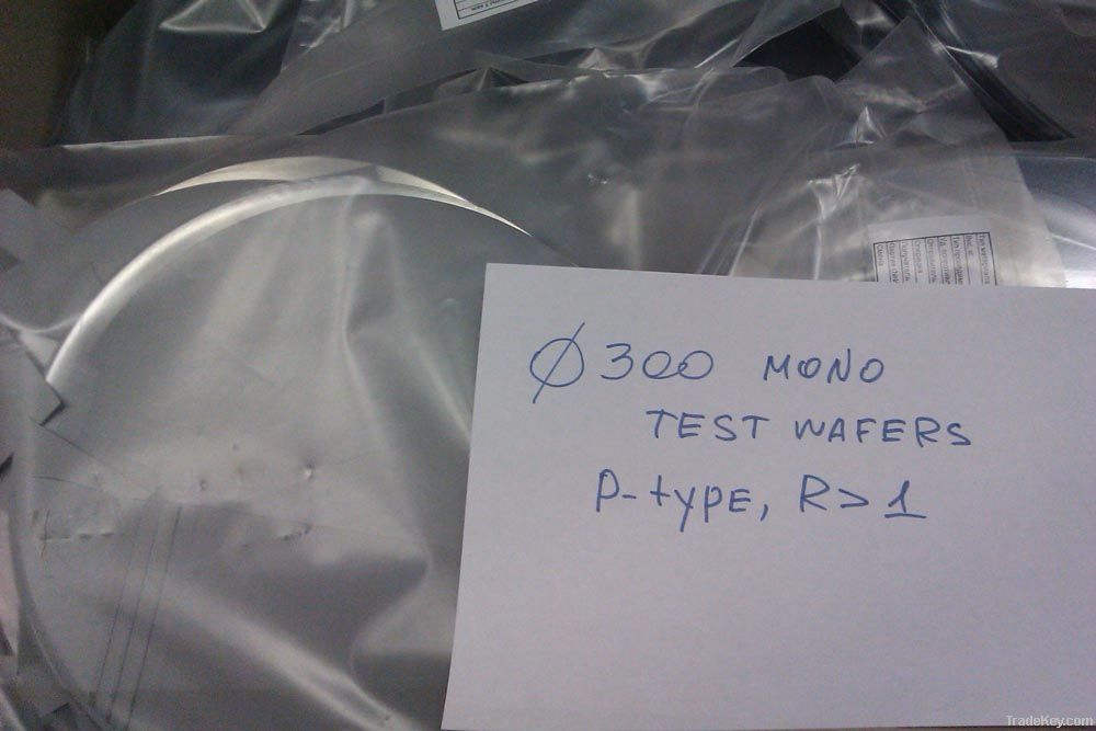
A wafer is a thin slice of semiconductor material, such as a
silicon crystal, used in the fabrication of integrated circuits and
other microdevices. The wafer serves as the substrate for
microelectronic devices built in and over the wafer and undergoes
many microfabrication process steps such as doping or ion
implantation, etching, deposition of various materials, and
photolithographic patterning. Finally the individual microcircuits
are separated (dicing) and packaged.
Wafers are formed of highly pure (*9.***9% purity),[1] nearly
defect-free single crystalline material.[2] One process for forming
crystalline wafers is known as Czochralski growth invented by the
Polish chemist Jan Czochralski. In this process, a cylindrical
ingot of high purity monocrystalline silicon is formed by pulling a
seed crystal from a 'melt'.[3][4] Dopant impurity atoms such as
boron or phosphorus can be added to the molten intrinsic silicon in
precise amounts in order to dope the silicon, thus changing it into
n-type or p-type extrinsic silicon.
The ingot is then sliced with a wafer saw (wire saw) and polished
to form wafers.[5] The size of wafers for photovoltaics is **0–**0
mm square and the thickness is **0–**0 μm. In the future, **0 μm
will be the standard.[6] Electronics use wafer sizes from **0–**0
mm diameter. (The largest wafer made has a diameter of **0 mm but
is not in production yet.)
| País: | Russia |
| N º de Modelo: | 2 |
| Precio FOB: | 18 / Kilogram Obtener el precio más reciente |
| Lugar de origen: | Germany |
| Precio de pedido mínimo: | 18 per Kilogram |
| Cantidad de pedido mínimo: | 1 Ton |
| Detalle de embalaje: | - |
| El tiempo de entrega: | 1 week |
| Capacidad de suministro: | 3 Ton per Month |
| Tipo de pago: | T/T, L/C |
| Grupo de productos : | - |


