

Precio FOB
Obtener el precio más reciente12 / Kilogram
|1 Ton Minimum Order
País:
Russia
N º de Modelo:
4
Precio FOB:
12 / Kilogram Obtener el precio más reciente
Lugar de origen:
Russia
Precio de pedido mínimo:
12 per Kilogram
Cantidad de pedido mínimo:
1 Ton
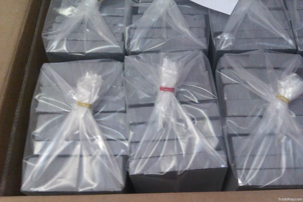
Detalle de embalaje:
-
El tiempo de entrega:
1 week
Capacidad de suministro:
21 Ton per Month
Tipo de pago:
T/T, L/C
Grupo de productos :
-

Russia
Persona de contacto Victoria
Olympisky prospekt, Mytishi
More recently, intrinsic and doped polysilicon is being used in
large-area electronics as the active and/or doped layers in
thin-film transistors. Although it can be deposited by LPCVD,
plasma-enhanced chemical vapour deposition (PECVD), or solid-phase
crystallization (SPC) of amorphous silicon in certain processing
regimes, these processes still require relatively high temperatures
of at least **0 °C. These temperatures make deposition of
polysilicon possible for glass substrates but not for plastic
substrates. The deposition of polycrystalline silicon on plastic
substrates is motivated by the desire to be able to manufacture
digital displays on flexible screens. Therefore, a relatively new
technique called laser crystallization has been devised to
crystallize a precursor amorphous silicon (a-Si) material on a
plastic substrate without melting or damaging the plastic. Short,
high-intensity ultraviolet laser pulses are used to heat the
deposited a-Si material to above the melting point of silicon,
without melting the entire substrate. The molten silicon will then
crystallize as it cools. By precisely controlling the temperature
gradients, researchers have been able to grow very large grains, of
up to hundreds of micrometers in size in the extreme case, although
grain sizes of *0 nanometers to 1 micrometer are also common. In
order to create devices on polysilicon over large-areas however, a
crystal grain size smaller than the device feature size is needed
for homogeneity of the devices. Another method to produce poly-Si
at low temperatures is metal-induced crystallization where an
amorphous-Si thin film can be crystallized at temperatures as low
as **0C if annealed while in contact of another metal film such as
aluminium, gold, or silver.
A polycrystalline silicon rod made by the Siemens process
Polysilicon has many applications in VLSI manufacturing. One of its
primary uses is as gate electrode material for MOS devices. A
polysilicon gate's electrical conductivity may be increased by
depositing a metal (such as tungsten) or a metal silicide (such as
tungsten silicide) over the gate. Polysilicon may also be employed
as a resistor, a conductor, or as an ohmic contact for shallow
junctions, with the desired electrical conductivity attained by
doping the polysilicon material.
One major difference between polysilicon and a-Si is that the
mobility of the charge carriers of the polysilicon can be orders of
magnitude larger and the material also shows greater stability
under electric field and light-induced stress. This allows more
complex, high-speed circuity to be created on the glass substrate
along with the a-Si devices, which are still needed for their
low-leakage characteristics. When polysilicon and a-Si devices are
used in the same process this is called hybrid processing. A
complete polysilicon active layer process is also used in some
cases where a small pixel size is required, such as in projection
displays.
| País: | Russia |
| N º de Modelo: | 4 |
| Precio FOB: | 12 / Kilogram Obtener el precio más reciente |
| Lugar de origen: | Russia |
| Precio de pedido mínimo: | 12 per Kilogram |
| Cantidad de pedido mínimo: | 1 Ton |
| Detalle de embalaje: | - |
| El tiempo de entrega: | 1 week |
| Capacidad de suministro: | 21 Ton per Month |
| Tipo de pago: | T/T, L/C |
| Grupo de productos : | - |


