Precio FOB
Obtener el precio más reciente0.5 ~ 1 / Acre
|999 Piece Minimum Order
País:
China
N º de Modelo:
-
Precio FOB:
0.5 ~ 1 / Acre Obtener el precio más reciente
Lugar de origen:
wuhan
Precio de pedido mínimo:
0.5 per Acre
Cantidad de pedido mínimo:
999 Piece
Detalle de embalaje:
Packaging according to customer requirements
El tiempo de entrega:
15days
Capacidad de suministro:
18000 Square Meter per Year
Tipo de pago:
D/P
Grupo de productos :
Persona de contacto Mr. lei
Building 3,Wuda hui Park, Road 1 Wuda Science and Technology Park , Jiangxia District, Wuhan city, H, Wuhan, Hubei
Remarks: the above quoted price is the actual quoted price of non - product, and the specific quoted price is evaluated according to your product drawingI'll give you the exact price!!!
Company introduction
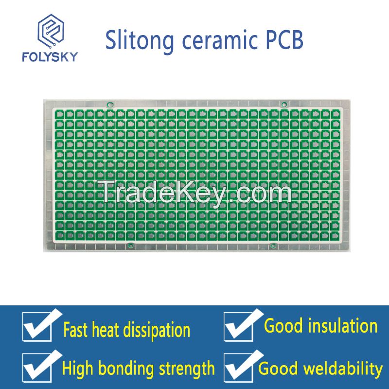
Decimating Skywin Technology (Wuhan) Co., Ltd., is a professional engaged in the plane and three-dimensional inorganic non metal based electronic circuits and electronic components research and development, production and sales of high-tech enterprises, which owns the well-known brand of ceramic circuit board *- Slitong.
The company's main products are ceramic circuit
board, such as alumina ceramic, aluminum nitride ceramic, zirconia
ceramic, glass, quartz, adopting metal technology of laser rapid
activation (Laser Activation Metallization, referred to as LAM)
production.- between the metal layer and the ceramic with high
strength, good electrical properties, can be repeated welding,
metal layer thickness can be adjusted within 1 m*1mm, L/S
resolution can reach *0 m, can be directly realized through holes
to connect, to provide customized production service for
customers.
The product has a number of patents in the development
and production process, technology has completely independent
intellectual property rights, the current annual production
capacity of ****0 square meters.
The company has professional production, technology
research and development team, advanced marketing management system
and high quality soft and hardware facilities. A systematic
decision process and a rigorous warehouse management system ensure
the efficiency of our production capacity. We are committed to
providing the most professional, fastest and most intimate
customized services to customers around the world.
Brand introduction -
Litong
As a leader in hi tech + Internet
mode, our company is committed to providing high quality products
and more intimate service to every customerCutting edge technology:
LAM technology, DPC Technology
Team Honors: Wuhan national
Optoelectronics Laboratory, Huazhong University of Science and
Technology R & D team, participated in international electronic
exhibitions several times
Close service: fast production
cycle, customized production according to customer's drawings
Brand core: focus on cutting-edge
technology, walking in the forefront of science and technology, so
that technology and products to grow together, the achievements of
different industry cutting-edge brands.
Process
introduction
LAM: our products by the national
invention metallization technology rapid activation of patent
(Laser Activation laser Metallization, referred to as LAM)
production, using ceramic and metal ion beam of high-energy laser,
so that the two are firmly combined. LAM technology can realize
large-scale production of single-sided, double-sided and 3D ceramic
circuit boards. The product has high precision and good adhesion,
and the conductive layer can be customized from 1 m to 1mm
according to customer's requirements. The use of pure copper
instead of silver paste can solve the problem of conductivity and
adhesion of the hole, and the overall performance is more stable.
The process is mature and the performance of the products is
excellent. High precision wiring can be achieved by laser incident
3D surfaces. Free from the appearance limit, the design space is
more imaginative, the cost is lower than the traditional
technology, no mold opening, environmental protection and
pollution-free, and the application field is extensive.
DPC Technology: thin film method is the main method of metal film deposition in microelectronic manufacturing, among which direct copper plating (Direct, plating, copper) is the most representative. Direct copper plating (DPC), mainly by evaporation and magnetron sputtering deposition process of metal substrate surface, first under vacuum sputtering of titanium, chromium and copper particles is, finally electroplating thickening, followed by ordinary PCB technology to complete production line, then the chemical plating / deposition increase line thickness.
| País: | China |
| N º de Modelo: | - |
| Precio FOB: | 0.5 ~ 1 / Acre Obtener el precio más reciente |
| Lugar de origen: | wuhan |
| Precio de pedido mínimo: | 0.5 per Acre |
| Cantidad de pedido mínimo: | 999 Piece |
| Detalle de embalaje: | Packaging according to customer requirements |
| El tiempo de entrega: | 15days |
| Capacidad de suministro: | 18000 Square Meter per Year |
| Tipo de pago: | D/P |
| Grupo de productos : | Ceramic circuit board |


Co., Ltd")


